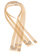
Endless application possibilities
Miniaturized flexible electronics offer great potential for medical, lighting and many more low-voltage applications. Examples include medical instruments such as catheters and endoscopes used in patient-friendly, minimally invasive procedures and energy-efficient, eco-friendly LED lighting surfaces integrated in building glazing.
Conventional cable wiring, however, comes with high manufacturing costs and high material consumption, while also restricting the scope of product innovation and performance improvement. These wiring limitations are addressed by the European HyPerStripes project, which aims to develop cost-effective technologies and production techniques for long, smart, flexible electronic systems (‘hyperstripes’) that can replace traditional cables and printed circuit boards. The stretchable hyperstripes are intended for providing long conductive tracks to electrical components.
Flexible, thin stripes with various hybrid electronic components integrated onto them do not incur any connection problems and can be manufactured long enough for, e.g., condition monitoring applications that may require meters of cables. In addition, new manufacturing techniques enable reduction in cabling thickness from as much as 35 µm to 1 µm, thus significantly lowering copper consumption. The HyPerStripes partners work on creating a technology platform and manufacturing techniques for roll-to-roll processing and integration of electronic components onto very long (‘endless’) flexible web substrates.
Meandering pattern
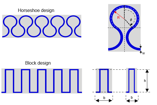
One of the main design challenges is the flexibility of the electronic cabling. Conductive materials such as gold, silver or copper usually are less strainable than the substrate material they are attached to. Substrates such as thermoplastic polyurethanes can accommodate up to 100% strain easily, while the maximum strain of conductors typically lies in the order of 10-40% (values for copper, depending on the production technique used). To increase the strain that can be achieved, the conductive tracks have to be arranged in a meandering pattern.
Conflicting requirements
Drawing up design rules for flexible electronics arranged in a meandering pattern is not straightforward, as there are conflicting requirements involved. Therefore, a simulation procedure for flexible systems was developed within the HyperStripes project. The focus was on reliability, to ensure cabling integrity, and sustainability, to minimize valuable conductive material content.
Integrity requires sufficient material to be present, as determined by width and thickness, while sustainability seeks to minimize these parameters. In turn, lower width and thickness increase the electrical resistance of the wiring, which is unwanted due to the heat generation that can affect, for example, human tissue. Adding to the complexity, making the wiring longer creates room for more flexibility but also increases the resistance. Ultimately, the design rules will reflect a trade-off between high strainability of the electronics product versus low wiring resistance.
Parametric finite-element models
This situation of conflicting requirements with respect to the various design parameters called for a systematic approach. From a mechanical point of view, the plastic strain in the conductive material was used as the critical parameter for assessing the ‘performance’ of a design up to failure of the system due to wire break. Building on its extensive expertise of material simulations, in particular of composite materials, Reden took up the challenge.
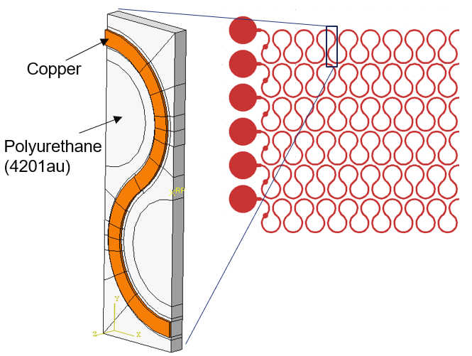
Reden decided to conduct Computer Design of Experiments (CDoE) to assess the strainability of the flexible conductors, using parametric finite-element models of the hyperstripes. To reduce simulation time, a unit-cell approach was used to represent a repeating part of the product. For two options, a horseshoe design and a block-shaped design, the influence of various design parameters was evaluated, while the materials involved were kept constant. These materials were polyurethane for the substrate and copper for the conductor, which is standard for industrial applications, while silver and gold are predominantly used in medical applications.
Modeling challenges
We had to dive into the copper material properties that we used as input to our simulation model. From literature, it was known that strain-stress curves for copper films display a high degree of variation depending on the way the copper has been produced. All copper varieties have a quite similar specific electrical resistance, but their mechanical properties can vary widely. We selected the most extreme curve, for electrolytically produced copper, that exhibits the highest stress levels and can withstand no more than 10% of strain. In this way, we ensured that our results would provide a lower boundary of the achievable strainability.
Another issue we had to deal with was the attachment of the conductor to the substrate. At first sight, a low-width, high-thickness wiring would yield good results in terms of strainability and resistance. However, low-width wiring may display poor attachment, which gives the risk of the conductor becoming detached (peeling) from the substrate. Here, the difference in stiffness between the conductor and the substrate also play a role.
To take this phenomenon into account, we paid special attention to modeling of the substrate-conductor interface, which may include intermediate layers to accommodate the delta in strain between substrate and conductor. For macroscopic applications, an interface model can be validated experimentally by double cantilever beam tests that characterize fracture in adhesively-bondedjoints. For thin-film electronics products such as hyperstripes, however, it is practically impossible to get a grip on both layers, which makes these tests not feasible. So, we could only use indirect measurement results to validate our model.
Wire thickness and width effects
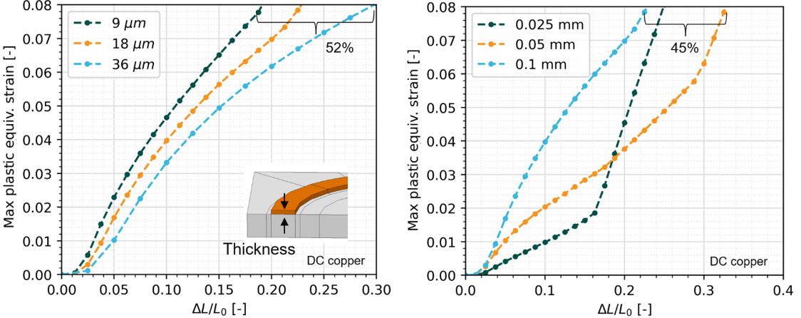
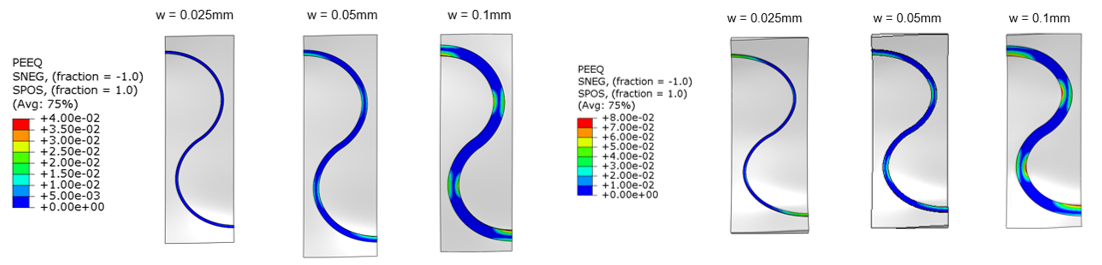
In our simulations, the plastic strain was determined as a function of the strain applied to the hyperstripe. As an illustration of the simulation results, the tensile test can be considered. For the horseshoe design different responses were observed depending on the wire thickness; the thickest wire was found to yield the most stretchable design.
When the wire width was varied, it was surprisingly found that the thinner wire initially exhibited better stretchability, but then showed rapid growth in plastic deformation. When looking at the wire geometry, the thickest wire was found to develop plastic strain in its mid-section due to bending effects,while the thinner wires mainly exhibited plastic strain around their tops in the large-strain case.
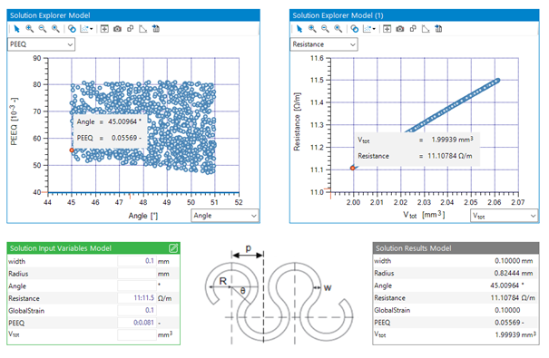
Design space exploration
To facilitate the creation of a design that fulfils the requirements, we have fed the CDoE results into our Reves Design Space Exploration (DSE) software. This software helps designers to explore the full potential of the design space and obtain better solutions faster, while also reducing physical testing and potential rework. For the HyPerStripes case, Reves DSE produces an overview of the relations between design parameters such as width, global strain, radius, resistance, curvature angle and PEEQ (plastic equivalent strain). For each graph, an input parameter and an output variable can be determined for which the results are displayed.
Now, the knowledge gathered in Reves DSE can be used to optimize the design of a hyperstripe product. For example, the design goal may be to keep the product cost as low as possible by minimizing the total amount of copper (Vtot) used. Then, in Reves DSE, boundary conditions can be set, such as a maximum value for the electrical resistance, to prevent unacceptable heat dissipation, and a minimum value for the strain that should be feasible. Other parameters, such as cabling width, can be set if desired, for example at a supplier-defined standard value. The Reves DSE exercise then yields a hyperstripe geometry that meets the design objective and boundary conditions. The output includes values for the remaining design parameters and the required amount of copper, which helps to give a cost estimate.
The results underline that the design of an optimal geometry for flexible electronics is far from trivial and simulations are definitely needed to produce realistic design rules. In the HyPerStripes project, we have demonstrated our capabilities to get a grip on physical phenomena in the microscopic domain and translate our understanding into robust models, which yield practical solutions for designers.